- 您现在的位置:买卖IC网 > Sheet目录1995 > DSD1792DB (Texas Instruments)IC 24BIT STEREO AUD DAC 28-SSOP
DSD1792
SLES067B MARCH 2003 REVISED NOVEMBER 2006
www.ti.com
20
High Impedance
When Read Mode is Instructed
A0
D7
D6
D4
D5
D3
D2
D1
D0
D7
D6
D4
D5
D3
D2
D1
D0
R/W
A1
A2
A3
A4
A5
A6
MS
MC
MDI
MDO
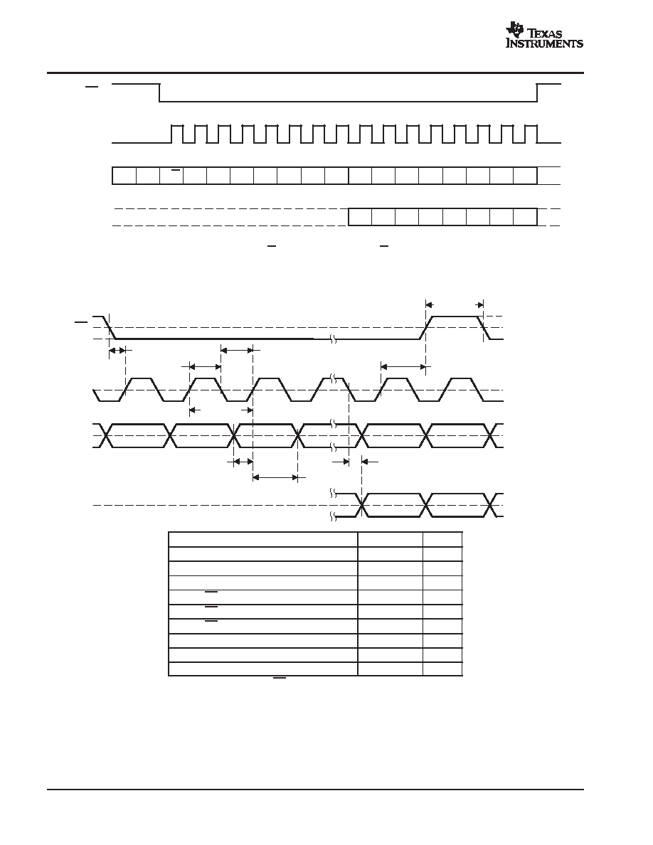
NOTE: Bit 15 is used for selection of write or read. Setting R/W = 0 indicates a write, while R/W = 1 indicates a read. Bits 14–8 are used for the register
address. Bits 7–0 are used for register data.
Figure 30. Serial Control Format
t(MCH)
50% of VDD
MS
t(MSS)
LSB
50% of VDD
t(MCL)
t(MHH)
t(MSH)
t(MCY)
t(MDH)
t(MDS)
MC
MDI
t(MOS)
50% of VDD
MDO
PARAMETER
MIN
MAX
UNITS
t(MCY) MC pulse cycle time
100
ns
t(MCL) MC low-level time
40
ns
t(MCH) MC high-level time
40
ns
t(MHH) MS high-level time
80
ns
t(MSS) MS falling edge to MC rising edge
15
ns
t(MSH) MS hold time(1)
15
ns
t(MDH) MDI hold time
15
ns
t(MDS) MDI setup time
15
ns
t(MOS) MC falling edge to MDO stable
30
ns
(1) MC rising edge for LSB to MS rising edge
Figure 31. Control Interface Timing
发布紧急采购,3分钟左右您将得到回复。
相关PDF资料
EL5001IRE-T7
IC CLOCK DRIVER 6-CHAN 20-HTSSOP
FT10001L6X
IC RESET TIMER 6-MICROPAK
FT3001MPX
IC RESET TIMER 8-MLP
FT7521L6X
IC RESET TIMER 7.5SEC 6MICROPAK
FT7522L6X
IC RESET TIMER 6-MICROPAK
FT8010UMX
IC RESET TIMER CONF DELAY 10UMLP
FTS125-COO-010.0M
IC GPS BASED TIMING MOD (OCXO)
FTS125-CTV-010.0M
IC GPS BASED TIMING MOD (TCXO)
相关代理商/技术参数
DSD1792DBG4
功能描述:音频数/模转换器 IC 24-Bit 192kHz Smplng Adv Stg Stereo DAC RoHS:否 制造商:Texas Instruments 转换器数量: 分辨率:16 bit 接口类型:I2S, UBS 转换速率: 信噪比:98 dB 工作电源电压:5 V DAC 输出端数量:2 工作温度范围:- 25 C to + 85 C 电源电流:23 mA 安装风格:SMD/SMT 封装 / 箱体:TQFP-32 封装:Reel
DSD1792DBR
功能描述:音频数/模转换器 IC 24-Bit 192kHz Smplng Adv Stg Stereo DAC RoHS:否 制造商:Texas Instruments 转换器数量: 分辨率:16 bit 接口类型:I2S, UBS 转换速率: 信噪比:98 dB 工作电源电压:5 V DAC 输出端数量:2 工作温度范围:- 25 C to + 85 C 电源电流:23 mA 安装风格:SMD/SMT 封装 / 箱体:TQFP-32 封装:Reel
DSD1792DBRG4
功能描述:音频数/模转换器 IC 24B 192kHz Sampl Adv Segment Aud St DAC RoHS:否 制造商:Texas Instruments 转换器数量: 分辨率:16 bit 接口类型:I2S, UBS 转换速率: 信噪比:98 dB 工作电源电压:5 V DAC 输出端数量:2 工作温度范围:- 25 C to + 85 C 电源电流:23 mA 安装风格:SMD/SMT 封装 / 箱体:TQFP-32 封装:Reel
DSD1793
制造商:BB 制造商全称:BB 功能描述:24 BIT 192 KHZ SAMPLING ADVANCED SEGMENT AUDIO STEREO DIGITAL TO ANALOG CONVERTER
DSD1793DB
功能描述:音频数/模转换器 IC 24-Bit 192kHz Smplng Adv Stg Stereo DAC RoHS:否 制造商:Texas Instruments 转换器数量: 分辨率:16 bit 接口类型:I2S, UBS 转换速率: 信噪比:98 dB 工作电源电压:5 V DAC 输出端数量:2 工作温度范围:- 25 C to + 85 C 电源电流:23 mA 安装风格:SMD/SMT 封装 / 箱体:TQFP-32 封装:Reel
DSD1793DBG4
功能描述:音频数/模转换器 IC 24B 192kHz Sampl Adv Segment Aud St DAC RoHS:否 制造商:Texas Instruments 转换器数量: 分辨率:16 bit 接口类型:I2S, UBS 转换速率: 信噪比:98 dB 工作电源电压:5 V DAC 输出端数量:2 工作温度范围:- 25 C to + 85 C 电源电流:23 mA 安装风格:SMD/SMT 封装 / 箱体:TQFP-32 封装:Reel
DSD1793DBR
功能描述:音频数/模转换器 IC 24-Bit 192kHz Smplng Adv Stg Stereo DAC RoHS:否 制造商:Texas Instruments 转换器数量: 分辨率:16 bit 接口类型:I2S, UBS 转换速率: 信噪比:98 dB 工作电源电压:5 V DAC 输出端数量:2 工作温度范围:- 25 C to + 85 C 电源电流:23 mA 安装风格:SMD/SMT 封装 / 箱体:TQFP-32 封装:Reel
DSD1793DBRG4
功能描述:音频数/模转换器 IC 24-Bit 192kHz Smplng Adv Stg Stereo DAC RoHS:否 制造商:Texas Instruments 转换器数量: 分辨率:16 bit 接口类型:I2S, UBS 转换速率: 信噪比:98 dB 工作电源电压:5 V DAC 输出端数量:2 工作温度范围:- 25 C to + 85 C 电源电流:23 mA 安装风格:SMD/SMT 封装 / 箱体:TQFP-32 封装:Reel